
Benefits and Setbacks of Surface Mount Technology (SMT)
In the ever-evolving world of electronics, Surface Mount Technology (SMT) continues to play a pivotal role in printed circuit board (PCB) assembly, shaping the future of communication, automotive, medical, and wearable technologies.
SMT, a technology that originated in the 1960s and gained widespread adoption in the 1980s, has become a staple in most high-end PCB assemblies by the 1990s. Today, SMT components, enclosed in a plastic mold and available in various shapes such as square or rectangular, are smaller than their through-hole counterparts, allowing for higher component density on the board.
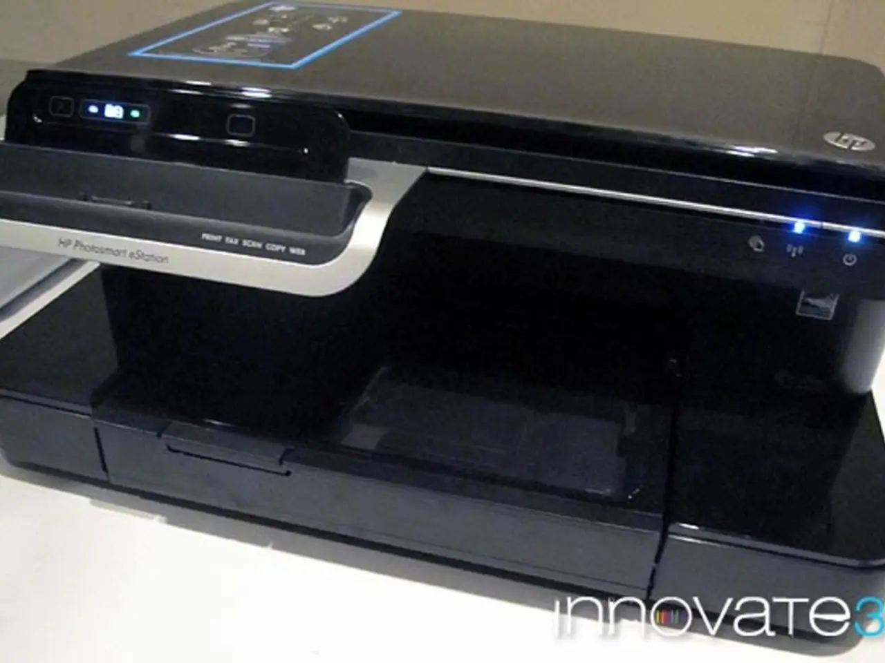
The compact size of SMT packages, such as SOIC, SOP, TSOP, QFP, and BGA, enables higher-density traces to be accommodated on the same layer, making it easier to achieve higher circuit speeds. SMT also allows electrical components to be mounted on the board surface without any drilling, streamlining the manufacturing process.
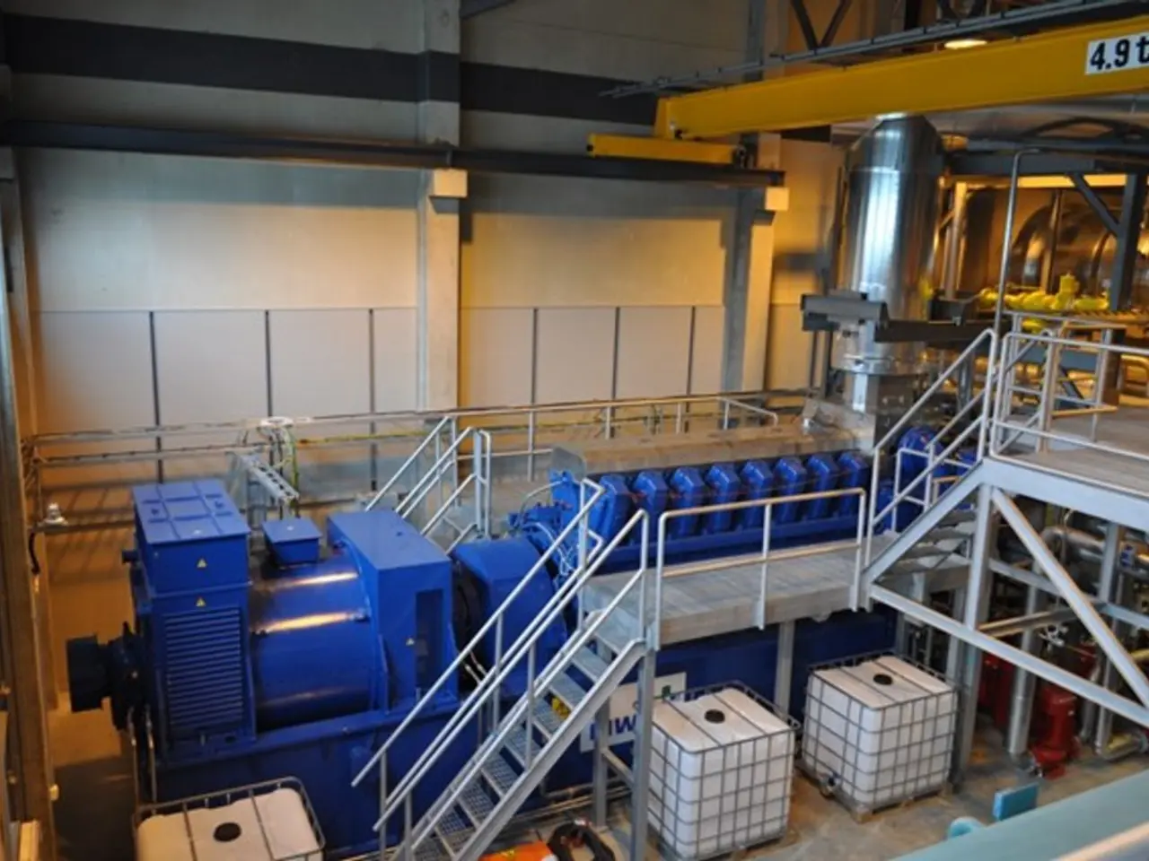
Recent advancements in SMT focus on increased automation, miniaturization, advanced materials, and integration with emerging manufacturing techniques. Automation technologies, including high-speed placement machines, robotics, automated optical inspection (AOI), and machine learning algorithms, are now heavily incorporated into SMT lines, boosting production efficiency and reducing labor costs.
Miniaturization is another key trend, with the use of extremely small components like 01005 (0.4 mm x 0.2 mm) and 02001 (0.5 mm x 0.25 mm) chip resistors and capacitors facilitating the production of smaller, lighter, and more compact devices.
Advanced materials and substrate technologies, such as ceramic PCBs with SMT, are gaining traction due to their high-temperature stability, excellent insulation, low thermal expansion, and robustness. These are essential for power electronics, high-frequency applications like 5G+, and electromagnetic compatibility.
Emerging manufacturing techniques, such as additive manufacturing and 3D printing, are transforming SMT by enabling the creation of complex geometries and embedded components within PCBs. Embedded components reduce device size and improve electrical performance.
Environmental and regulatory trends also play a significant role in SMT advancements, with lead-free, eco-friendly soldering and recyclable materials increasingly adopted to meet environmental regulations and sustainability goals.
SMT dominates the PCB assembly market with approximately 75% market share in 2025, favoured for its ability to support high-density component placement and automated mass production. Mixed technology assemblies that combine SMT and through-hole components are also growing due to complex design requirements, especially in automotive and industrial sectors.
However, it's essential to understand that SMT is not suitable for all cases. It is best suited for accommodating a high density of components, producing compact or small products, creating sleek and lightweight devices despite component density, supporting high-speed/frequency functioning of the device, producing large quantities with automated technology, and producing devices that produce very little noise (if any at all).
In summary, the latest SMT advancements emphasize automation, ultra-fine precision, miniaturization, ceramic PCB integration, embedded components, and sustainable manufacturing practices, enabling the production of more complex, reliable, and compact electronic devices needed for next-generation communication, automotive, medical, and wearable technologies.
SMT components, smaller than their through-hole counterparts, have become essential for achieving higher component density on the board, shaping the future of communication, automotive, medical, and wearable technologies. In advanced manufacturing lines, automation technologies and machine learning algorithms are now heavily incorporated into SMT lines, boosting production efficiency and reducing labor costs, marking a significant trend in SMT advancements.


)