YouTuber Robert Feranec Makes a Trip to Sierra Circuits
In a recent visit to Sierra Circuits, YouTube PCB designer Robert Feranec gained insights into the company's PCB manufacturing and assembly services. The 40-page Design for Manufacturing Handbook, a comprehensive guide offering best practices for trace width and space, annular rings, and optimizing vias, among other topics, played a significant role in the tour.
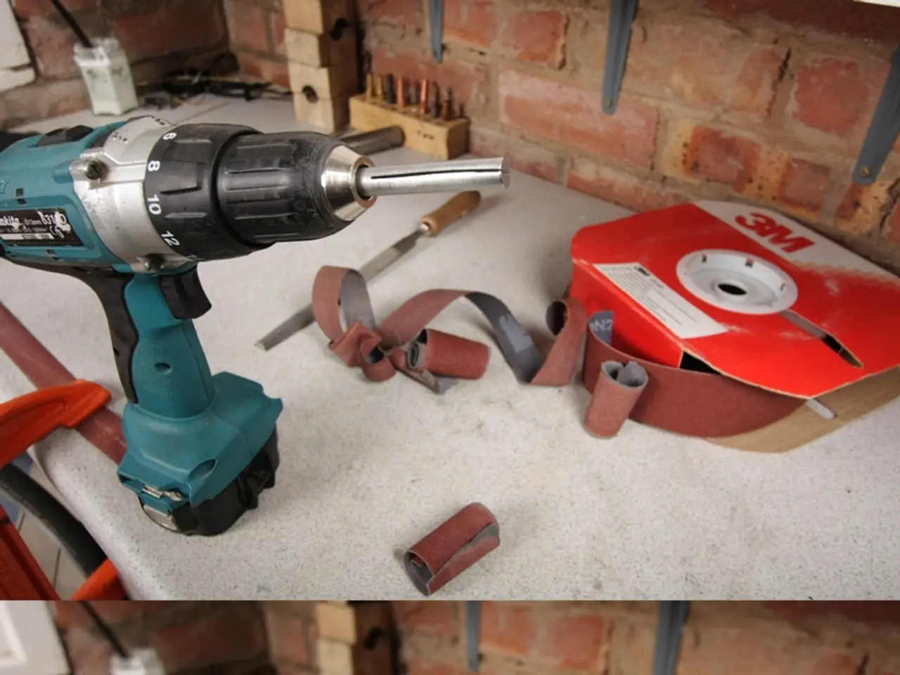
The Handbook, a 45-minute read, provides must-knows about solder mask and silkscreen, and is divided into 10 chapters. During the tour, Feranec was amazed by several techniques demonstrated, including the drilling process.
The video, featuring various aspects of the PCB manufacturing process, offers a detailed look at the drilling area, slivers, teardrops, etch compensation, wires, copper, thermal relief, 45 and 90 degree angles, small copper dots, prepregs, thermal stress, baking PCBs, drilling, mask over VIAs, assembling boards, minimum distance between two holes, checking the Gerber files, plating microvias, the coupons, and the price of a PCB.
Feranec's visit highlighted a thorough, hands-on approach starting from schematic design, footprint verification, and PCB layout through to manufacturing preparation. Key points included accurate schematic drawing and component selection, consistent track width for signal integrity, precise component placement, 3D model verification, importing schematic changes to PCB layout, ordering manufacturing files carefully, and the use of professional tools and libraries.
Moreover, Feranec's process implied attention to design for assembly (DFA) considerations, including footprint sizes and pad design to facilitate soldering and assembly, and surface-mount technology (SMT) best practices.
Feranec's focus on teaching through clear tutorials that cover hardware design, PCB layout, and production from start to finish, often including practical tips on troubleshooting and EMC considerations, was evident in his demonstrated approach with Sierra Circuits. This approach can be summarized as a structured, detail-oriented workflow focusing on robust schematic capture, precise layout with manufacturability in mind, verification via 3D models, and clean data preparation for PCB fabrication and assembly.
Amit Bahl, the director of sales and marketing at Sierra Circuits, showed Feranec the manufacturing and assembling process from start to finish, leaving Feranec amazed by several techniques demonstrated during the tour, including the drilling process.
[1] Robert Feranec's Tutorials: [Link to tutorial] [2] Sierra Circuits: [Link to Sierra Circuits website] [3] Design for Manufacturing Handbook: [Link to Handbook] [4] Robert Feranec's Content: [Link to content] [5] EMC Considerations: [Link to EMC resource]
- Robert Feranec's visit to Sierra Circuits showcased his interest in gadgets, as he gained insights into the company's PCB manufacturing and assembly services, and was particularly impressed by the demonstrated drilling process, which is a key aspect of technology involved in the PCB manufacturing.
- The Design for Manufacturing Handbook, a resource provided by Sierra Circuits, offers valuable information about various aspects of PCB manufacturing technology, including solder mask and silkscreen, drilling, and assembly, making it a must-read for anyone interested in gadgets and technology.


